Material innovations for wafer-level packaging technologies
| Focus topic: | Resource efficiency |
|---|---|
| Type of funding: | Project funding programmes |
| Programme: | CZS Transfer |
| Funded institution: |
|
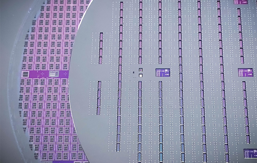
Wafer-level packaging is a chip manufacturing technology. It increases integration densities and reduces the use of materials and energy. The project aims to bring new material concepts and 3D printing technologies to production maturity.
Goals
In wafer-level packaging (WLP), the assembly steps of semiconductor chips into ready-to-use components, such as encapsulation and contacting, take place simultaneously and directly at wafer level. In contrast to conventional production, the semiconductor wafers are processed significantly further before being separated into separate chips. The new technology thus significantly reduces the component size, accelerates and bundles production in one factory and reduces the use of materials and energy. In the project led by Prof. Roy Knechtel and Dr. Martin Seyring, various potential processes and material systems are being combined at Schmalkalden University of Applied Sciences. The aim is to bring the process into industrial production.
High-performance wafer bonding systems and solderable metallizations are being developed for the WLP - both based on resource-saving thin-film systems. Innovative 3D printing technologies are used for structured deposition at wafer level. The solutions are designed to minimize the use of materials and energy. Environmentally friendly, recyclable process chemicals are used. The project team is also developing a concept for technology transfer to industry.
Involved persons:

Prof. Dr.-Ing. Roy Knechtel
Hochschule Schmalkalden
Detailed information:
| Focus topic: | Resource efficiency |
|---|---|
| Programme: | CZS Transfer |
| Type of funding: | Project funding programmes |
| Target group: | Professors |
|---|---|
| Funding budget: | 1.000.000 € |
| Period of time: | März 2024 - Februar 2027 |
Funded institution:
